


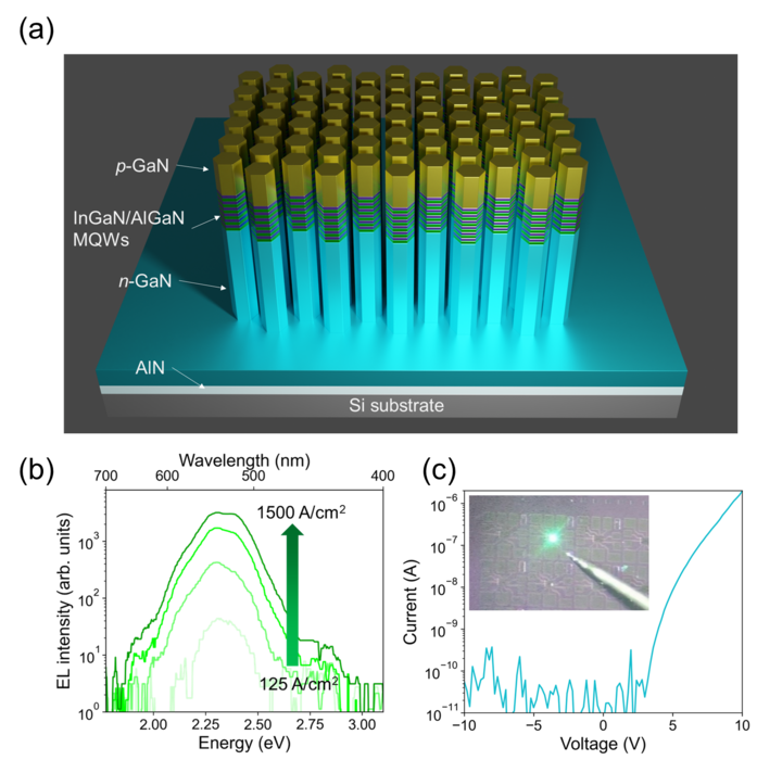
IMAGE: (A) SCHEMATIC OF THE INGAN/AGAN MULTIPLE-QUANTUM-WELL NANOWIRE ARRAY. (B) THE PEAK WAVELENGTH OF THE DEVICE’S ELECTROLUMINESCENCE STAYS CONSTANT OVER ONE ORDER OF MAGNITUDE OF CHANGE IN CURRENT INJECTION. (C) THE CURRENT VOLTAGE CHARACTERISTICS OF A DEVICE THAT SHOWS GOOD RECTIFICATION RATIO AND STRONG GREEN EMISSION VISIBLE TO THE EYES.
CREDIT: BY YUANPENG WU , YIXIN XIAO , ISHTIAQUE NAVID , KAI SUN , YAKSHITA MALHOTRA , PING WANG , DING WANG , YUANXIANG XU , AYUSH PANDEY , REDDEPPA MADDAKA , WALTER SHIN , JIANGNAN LIU , JUNGWOOK MIN, ZETIAN MI
Due to their superior properties in efficiency, stability, and device volume, conventional light emitting diodes (LEDs) have already revolutionized the lighting and display world. LEDs are typically stacks of semiconductor thin films with lateral dimensions on the order of millimeters, which are much smaller than traditional devices such as the incandescent light bulbs and the cathode tubes. Yet, emerging optoelectronic applications such as virtual and augmented reality demand LEDs with dimensions on the scale of micrometers or smaller. It is desired that the micro or submicron scale LEDs (µLEDs) continue to possess the many superior qualities that conventional LEDs already do, such as highly stable emission, high efficiency and brightness, ultralow power consumption, and full-color emission, while being about one million times smaller in area, allowing for much more compact display. Such µLEDs would also pave ways for much more powerful photonic circuits if they can be monolithically grown on Si for integration with complementary metal-oxide-semiconductor (CMOS) electronics.
To date, however, such µLEDs remain elusive, especially in the emission wavelength range of green to red. The conventional approach to µLEDs is a top-down process in which InGaN quantum well (QW) thin films are patterned into devices with dimensions in the microscale via etching processes. While thin-film InGaN QW-based µLEDs have attracted much attention due to many desirable properties of InGaN such as efficient charge carrier transport and wavelength tunability across the entire visible range, so far they have been suffering from issues such as sidewall etching damage that worsens as the device size shrinks. Further, they suffer from wavelength/color instability due to the polarization fields, for which solutions such as non-polar and semipolar InGaN and photonic crystal cavities have been proposed but have been unsatisfactory so far.
In a new paper published in Light Science & Application, researchers led by Professor Zetian Mi from the University of Michigan in Ann Arbor, USA, have developed III-nitride submicron-scale green µLEDs that overcome these barriers all at once. These µLEDs are synthesized with selective area plasma-assisted molecular beam epitaxy. In stark contrast to the conventional top-down approach, the µLEDs here consist of arrays of nanowires, each of which is only 100~200 nm in diameter and tens of nanometers apart. Such a bottom-up approach intrinsically avoids sidewall etching damage.
The light emitting part of the device, also known as the active region, consists of a core-shell multiple-quantum-well (MQW) structure that is unique to the nanowire morphology. In particular, the MQW consists of InGaN wells and AlGaN barriers. Due to differences in adatom migration on the sidewall between the group III elements of indium, gallium, and aluminum, indium is found to be absent on the sidewalls of the nanowire, where a GaN/AlGaN shell wraps the MQW core like a burrito. The researchers have found that the Al content of this GaN/AlGaN shell decreases from the electron injection side to the hole injection side of the nanowire. Due to the difference in internal polarization field between GaN and AlN, such a bulk gradient in Al content in the AlGaN layers induces free electrons, which can easily flow into the MQW core to alleviate the color instability by mitigating the polarization fields.
Indeed, the researchers have found that the peak wavelength of electroluminescence, or electrical current-induced light emission, remains constant over one order of magnitude of change in current injection, for a device with a diameter less than one micrometer. Moreover, Prof. Mi’s group has previously developed a method for growing high-quality GaN epilayer on silicon, on top of which the nanowire µLEDs are grown. As such, the µLEDs sits natively on a Si substrate, ready for integration with other CMOS electronics.
Such µLEDs readily have many potential application scenarios. The device platform would become more robust with the extension of emission wavelength into red for on-chip integrated RGB display.
Post time: Nov-01-2022